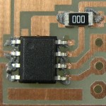
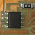
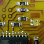
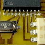
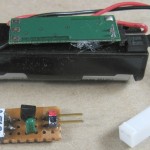
Jim Harvey and I got together at the space 2/16 to test and install the first 6 columns’ worth of latch boards. First step was to test them. That was a very good idea, since there were some bad traces I’d forgotten to fix. It would have been really annoying to discover the problems only after the boards were soldered into the display!
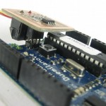
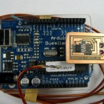
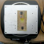
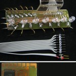 I made up a sort of ‘bed of nails’ tester that allows an Arduino to power and drive the inputs to the latch, and connects LEDs to its outputs to see the results. I needed 7 data bits in (for the 7 LEDs in the latched column), a clock, and of course power and ground. Trying to simplify the connections to the Arduino, I chose to use D0-D7 for the 8 data bits, since they’re all on one header. Since Do/D1 are the serial I/O pins, I can’t use serial I/O while using this tester. Setting those pins as output does allow them to be used for normal I/O, though.
I laid the board out by starting with the latch board layout and putting pads to solder the ‘nails’ to as wires or rectangles on another layer. When they looked like they were in reasonable places, I deleted the normal top and pad layers that made up the real board.
The first oops was that I pictured the LEDs on the non-foil side of the board, but laid the solder pads out so the foil was on top. Fine, so the LEDs will sit up in the air. I figured bending all the pins (0.025″ square pins salvaged from some old wire wrap board) would be a hassle, and I was right. I got them pretty close, and Jim H lapped them on some emery paper and got their tips a little closer to coplanar.
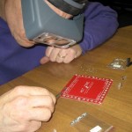
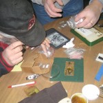
Second oops was when I realized we’d need a handle to press the tester down on the board under test. I bent a little acrylic handle and epoxied it on, but located it where it was  convenient instead of where it needed to be: You have to put pressure at sort of the geographic center of all the pins, not over where I glued the handle on. Shoulda seen that one coming. We ended up just pressing on the board with fingers to try to make all 17 contacts at once. Here’s Jim trying to do that (and ignoring the handle).
The arbitrary test pattern code did 2 cycles of cylon 1 LED-at-a-time sweeps, followed by 2 cycles of alternate LEDs on. The latter was a test that the latch actually latched, as I wrote the data, kicked the clock, then wrote zeros of data before sleeping. The code didn’t work first try, as I’d reordered a couple of pins as a tradeoff in the PCB layout but forgot to do it in the code. Here’s a clip of what it looks like with the final code and when you actually get all the contacts to make on a good board: LatchTester1
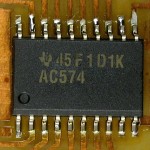
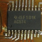
 Of course all the boards didn’t work first try. (That’s why we test!) We found a few bad (reflowed!) solder joints, which I fixed using solder-loaded braid to apply solder. Jim found some hairline disconnects in some traces by inspecting very closely. We soldered fine wires across those, and finally got all the boards working. Time to install!
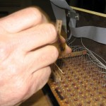 Jim had made a little jig he hoped would help hold the boards in place while we soldered their big pads to the LED
 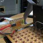 anodes. It turned out we could hold them quite well with one just clothes pin (which Jim had cleverly brought along), so we ended up doing that. Here’s the first board soldered in place:
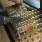 We hooked it up with the latch tester code and sure enough, the first column of LEDs in the display danced the tester dance. Encouraged, I put the other 5 boards in. Here’s a picture of soldering in the data bus that provides parallel data to all the boards. Yes, it’s labor intensive.
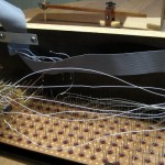 The original design had four 74154 1-of-16 decoders providing an (active low) column select. We planned to use that to clock the latches. Here’s the first crude wiring of those latch clocks. Unfortunately – probably partly because we digitalWrite() the address bits out one at a time – the latches don’t reliably latch the correct data. (As the address bits change one by one the 74154 selects probably go active on unintended columns. And running fast TTL pulses on those loose wires is asking for trouble as well!) So while the LEDs flashed around with all 6 boards in place and a simple scrolling pattern in the Arduino driving it, they clearly didn’t do what they were supposed to do.
So the next step is troubleshooting the addressing/latch clocks. I have a little USBee logic analyzer that would let us look at what actually shows up on the select lines, but I’m kind of afraid we’ll need to come up with a whole new 1-of-64 addressing scheme that guarantees clean clocks. I won’t even bother to make up any more latch boards until we can demonstrate that we can get those good clock pulses.
Update 2/17/12: Oops – tests of all 6 boards were invalid. I forgot to provide power to the 74154s in the display box! It’s always nice when finding out your tests were invalid is a good thing.
We should be able to provide clean 6-bit addresses to the ‘154s if we use 6 bits of 74373/4 octal latch to buffer the bit-by-bit changing address the Arduino puts out and clocking it out when we’ve written all 6 bits. That’s a pretty simple hack, and I even have some ‘373s and ‘374s.
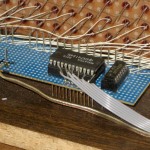 Update 2/28/12: Went to the space 2/23 and after Eric’s excellent Christmas (and Halloween) light display talk, made some good progress. First was rewiring the 6 input lines to the ‘154 board. I chopped down the silly long ribbon cable, kept the 6 pin male end, and connected nicely to the pins on the blue board.
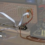 Next was a more proper power interconnect. A terminal block to connect to an external supply now powers both the 154 board and the latch boards (and their LEDs). (Schlocky picture, but that’s how we learn.) A little hot melt and it all stays in place.
With the cabling a little more sensible, I tested using a direct port write to change the state of all 6 address lines at once (instead of writing several invalid addresses as the bits changed one by one with digitalWrite()). After several rounds of fixing stupid coding, it almost worked! The first hard coded pattern was just 2 sawtooths (sawteeth?) scrolling in opposite directions. But column 1 just kind of sat there with a couple of LEDs always on. Investigation showed that when we were inspecting the boards for bad traces, on the board with visible lengthwise hairline opens, we fixed the traces for data, but ignored the fact that the opens went thru the clock pad. When I soldered the clock line to the pad, Murphy made me solder to the part separated from the trace that went to the chip. It just barely worked (but worked well enough the first night that Jim and I both watched correct patterns on all 7 LEDs). Then while we weren’t watching, it failed. I resoldered the clock line to the side of the pad connected to the chip, and it worked fine. Here’s a clip. Sorry about the orientation. I wasted way more time than I should have trying to fix it. (I could rotate it but then couldn’t fix the aspect ratio.)
Encouraged, I hand coded pixels for “W88”. Here’s a clip. It’s not perfect (the display – we know the clip is sideways and crappy), but it’s pretty clearly working. Some columns sort of fade and blink. That’s the real display, not a video artifact.
The interesting surprise is that the low resolution (7 pixels vertical and 0.5″ pixel pitch) makes the display kind of disappointing. I suggest making up (and testing and installing) maybe 10 more boards so we can get at least a minimal idea how it will actually look. At that point we can make the call whether it’s worth all the effort to populate the other 48 columns. It will definitely have a ‘retro’ look, but I don’t know whether that will save it from just looking kind of pathetic. That evaluation is for a little later.
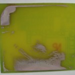
So we have an INPUT of a chip that can somehow pull the active output of a 154 down enough to make a visible difference in an LED. And that board never lights its target LEDs as bright as it should, and doesn’t always latch data in (or at least doesn’t display it on its 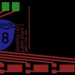 output LEDs). What kind of failure or short on the board could make the clock input draw a lot of current? Sorry, didn’t feel the temperature of the chip – shoulda. And it doesn’t always pull a high level down – apparently only when it has to light its LEDs. The only test pattern we’ve looked at is all LEDs on. It would be interesting to see if it was less bad for fewer LEDs. For reference, here’s the board layout.
OK – what if the chip wasn’t getting power and was effectively being powered by current drawn into that clock input? Is that even possible? High draw from a bunch of LEDs (in addition to powering the chip itself) might well pull that 154 output down. I guess those are the next things to look at. Unfortunately, I don’t have a spare board (yet) to explore behaviors like that.
Trying to get a board out from the middle (boards in place on both sides) with the data bus laid into slots on the top of the board will be a challenge. It would be embarrassing if it was just a cold solder joint on the +5 line for that board, but I guess that would be better than having to pull the board out.


