
Background failures
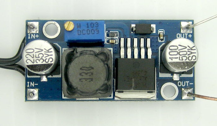
I’ve had some problems getting DC power for the audio amp for the starter’s gun project. I needed maybe 15V to get the output I needed, but didn’t want a battery voltage that high, so looked at boost converters. I found some little (Chinese) boards for $2.50 on Ebay that took in 1.2V or more and put out what ever you wanted up to 30V or so, and said 4A max. Should be fine, and I can’t even source the parts for that money. I ordered some.
Running off one 3.7V 18650 Li-ion cell they put out 15V no problem. The first surprise was that when I put it all together, the whole thing didn’t work. Funny noises from the speaker, and the Tiny4313 wouldn’t even boot reliably. It took a while to figure out I was running afoul of the current limit of the protection PCB in the cell. (Worked fine with the unprotected 2P bench battery!)
While the design had been for one 18650, in desperation to get a prototype working, I put in 2 cells in series. Sure enough, now the Tiny booted, no funny noises, and it played sounds, though not quite as loud as I expected. I looked at the voltage out of the converter with a scope, and during loud sounds it dropped from 15V to ~8V! WTH?!? Going thru the doc more carefully, that was 4A max input current, and there are limitations of max output current at various output and input voltages. Rats.
Very grudgingly, I decided to try a small 12V sealed lead acid battery. Surely the boost converter will do what I need with that much voltage in. But this time I’ll actually measure and qualify the boost converter at 12V in / 15V out. Let’s see – I may need 2A (or a little more?) at 15V, so I need a resistor to provide that load. Whoa – that’s 30 or 40 watts. Using a 2W 10Ω resistor – and just at 1.5A – the resistor got really hot before I could even comfortably make measurements. Sure would be nice if I had that high power adjustable current sink I’ve thought about making from time to time. And that need brings us up to this yak-shaving project.
The current sink
Electronics
A current sink is basically a big honking transistor with a big honking heat sink, plus some electronics to let you control how much current it will sink. I should be able to come up 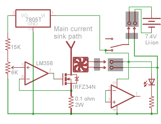 with that out of the junk box. A little googling scored ideas that led to this as the final design: (Bonus: I figured out how to add an image to a custom library schematic symbol in Eagle!)
I found an N-channel MOSFET good for max 55V and 29A – sounds fine. A 0.1Ω current sense resistor under it provides feedback thru an op amp listening to a pot for a reference voltage (and thus current). I went with using the bench 2S Li-ion battery for the occasional use this device will get, as the spec sheet indicated the MOSFET wouldn’t turn on for many amps without > 3.7V on the gate. A voltage regulator feeds the reference pot for stability. The heat sink has a 12V fan, which runs fine (and quietly) on 8V. A switch, an LED and a couple of resistors (for LED and pot range set) plus some connectors and it should work!
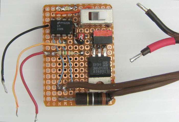 It looked simple enough that I could get away with perfboard instead of making a PCB. It took longer than I hoped, but it came out OK. The lampcord is for the current to be sunk. There’s a 2-pin 0.1″ male for power in and a 2-pin female for power to the fan. The 0.1Ω resistor is across the bottom. Its long left lead
 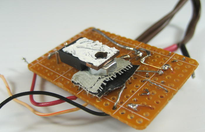 is to clip a voltmeter to for setting the current (0.1V/A).
The only mildly clever bit was using some gaffer’s tape to hold the nut in place while assembling it to the heat sink. Worked well and pulled out easily. I had to grind one side of the nut down so the hole would line up.
Heat sink
I’ve never really done any proper thermal management design, so the heat sink was new territory. Fortunately, Dave has a simple intro to heat sink basics on EEVblog that got me started. Thermal resistance of a heat sink in °C/watt makes perfectly good sense. But who knows what the TR is of all the random stuff in the junk heat sink box?
I looked around in Digikey to get some ballpark numbers. The heat sinks there ranged over 3 orders of magnitude – from 0.1 to 100°C/W. Reasonably enough, the 100°C/W jobs were tiny fins you could glue to a DIP, and the ones at the other end were massive CPU coolers with fans and heat pipes. The one Dave used was ~5°C/W with no fan. If I could get to maybe 2°C/W with a fan, the 60C increase at 30W would hit ~85C – well within the operating temp of the transistor. Might work!
 To be conservative, I grabbed the biggest sink I could find, and peeled the old Pentium off the bottom. Unfortunately, since it was designed for the large flat top of the processor, there were no holes in it to mount the TO-220 MOSFET. Drilling thru the fins for the nut or screw head would be a pretty ugly task. Maybe if I had a 1/2″ end mill – but I don’t. I suppose there might be one at the space, but that has problems of its own. Bummer.
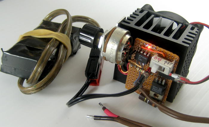 The next biggest was much smaller, but had fins that allowed drilling a mounting hole – sold! Here it is attached to the finished device. (The MOSFET is on the underside of the perfboard.)
On the to-do list is putting a temperature probe on the transistor and characterizing time/temperature/power curves with and without the fan. Sure would be nice if I had that datalogger I’ve been thinking about making…
“Opportunities for improvement”
While the current sink was a junk box special, I did try to think it through. For example, I wanted to be able to run with or without the fan. But did I really need another switch? Naw – the 2 pin connector would be fine. Did it really need an LED? Yeah, I could imagine accidentally leaving it on. And I dry fitted the parts to make sure it would all go together. But I still had 2 surprises – one electrical and one mechanical.
The main consideration in something like this is handling the power – and getting rid of the attendant heat. I put some moderate effort into the heat sink to do that. If it can dump 30 W or more without the transistor going above maybe 85C, it should be fine. The MOSFET is good for 29A, so current isn’t a problem.
Well, not for the transistor. But what about that 0.1Ω current feedback resistor? I’d like to be able to do 10 or 20 A. But wait – at 10A that resistor will dissipate 10W! With the 2W resistor I used, it’s only good for ~1.5A. Boo. I ordered some 20W 0.1Ω resistors to upgrade it some day. 0.1Ω resistors don’t usually manage to get very hot, but I guess this isn’t a usual application!
The mechanical issue was pretty bad, and I really should have seen it coming. The only mechanical connection between the heat sink and the perf board is the MOSFET – or more accurately the 3 legs of the MOSFET’s TO-220 case. To allow for some air flow past the transistor, it’s 1/4″ off the board – with only those spindly legs in between. The pot – which is manipulated a lot – is screwed to the heat sink – so that’s not a problem. But the power switch and the connector for the battery are on the perfboard. And every time I touch either one, the board woggles around dangerously.
There’s a nice chunk of aluminum very near by, and I could drill and tap a hole for a screw. But I don’t have much real estate left on the board, and if I used a plastic spacer I’m not sure how it would do with a hot heat sink. I’m sure I’ll come up with something, but  catching it earlier would have been good.
Update (next day): OK, this is crude, but it keeps the board a lot more stable, particularly when I operate the switch. Good enough.
Update 11/8/17: The $150 Basement Watchdog brand battery 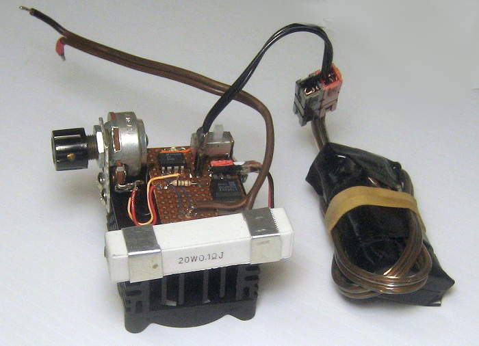 for the backup pump installed 2/17 seems to be bad. WTH? I wanted to do a discharge test on it, and the current sink seemed appropriate, but the 0.1Ω current sense resistor would limit the discharge rate. It’s finally time to put one of those 20W jobs in.
Mechanical mounting is fine, though I’m not proud of the blob-of-solder electrical connections. But it looks like it works. I used the new bench supply and ran up to ~5A. The voltage side of the supply was set to 8.7V, so it was drawing ~50W. The power supply fan – which I’ve never heard before – came on promptly. I adjusted the sink for about 3A just so the supply wasn’t at one of its limits. The current sink’s heat sink was quite warm (its fan, powered with the 7.4V bench battery, was on). When I turned the voltage down to ~0.5V, the current (voltage across the sense resistor) stayed just about constant, and the power supply’s fan went off. Looks like it’s all doing what it should!
Back to the task at hand
 Now to take a closer look at the little boost converter. I don’t know how it works, but I wonder if a larger cap on the output would help keep the voltage from drooping? Hmm – looking at the board, the larger cap in on the input. Is that just another student error? These things are usually exactly from the example schematic in the datasheet. Let’s see…
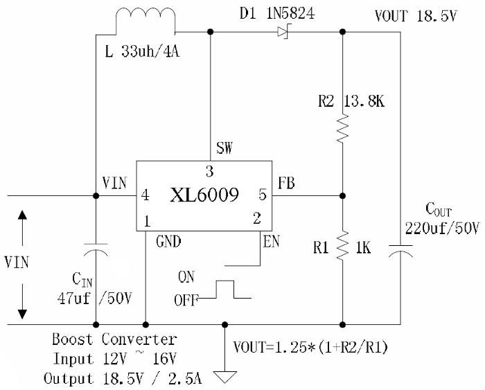
Gee – it shows a 220μF on the output – and the board has a 220 on the input. Pretty suspicious.
Ooh – a shiny thing to distract me!
Looking at the schematic, I realized I had no idea how this thing worked. OK – output cap, voltage divider on the output for feedback, some kind of enable, yeah, yeah. And all the current that goes to the output goes thru the inductor. Oh – except for what comes from that “SW” pin. What does that do? <checks block diagram in datasheet>
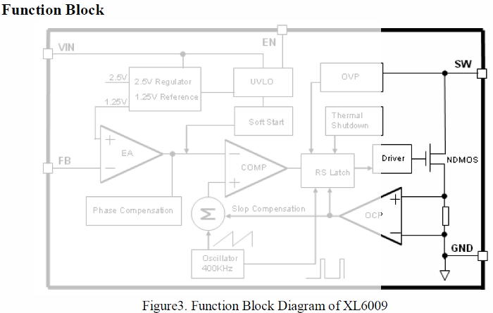 Hmm – nuthin’ comes out of that pin. All it has is a MOSFET to ground. So all it does is … SHORT OUT THE INPUT AND OUTPUT TO GROUND! WTH?!? Oh, that’s what the diode is for: it doesn’t short out the output. But it still shorts the input to ground! OK – thru the inductor, but still…
<light slowly comes on> OK, as soon as the switch comes on (connects to ground), the whole input voltage is impressed across the inductor. There’s no current spike – since the inductor “doesn’t want the current to change”. But as the current slowly builds, it’s storing energy in the inductor. When the switch opens, the current thru the inductor would drop, but there’s a big inductive spike as the inductor keeps the current flowing. Where does it go? (Thru the diode and) into the output cap! Aha!
So what does that inductor-driven ripple look like? And is it better/smaller with more capacitance across the output? <hooks output to the new current sink and puts scope across the boost converter output>
 Here’s the output voltage (AC coupled, 20mV/div, 1μs/div) at 0.5A stock (left) and with another 100μF across the output. <scratches head> So maybe with more C there’s lower impedance to the high frequency component of the inductive spike, and we see it as a leading spike on output voltage? I’m really not sure how it’s all supposed to work, but there’s a gut reaction that says those near-square waves from the stock config indicate that the inductor and stock cap are about ideally matched, despite the 220μF value in the datasheet example.
I suspect the tilt in the stock picture is the cap being discharged at constant current. Let’s see: Stackexchange says discharging a cap at constant current gives a rate of voltage change of I/C v/sec. That’s 0.5A/100μF=5V/ms, or 5mV/μs. Eyeballing the 2 slopes of the waveform (bottom is steeper), it’s maybe 0.25div vertical per div horizontal. At 20mV/div, that’s 5mV; horiz is 1μs/div; so that’s about 5mV/μs!
 Hmm – so if I change the current load, the slope should change. <goes back to bench> Well that was interesting. Here’s the output ripple at 100mA and 800mA. Starts with the bottom flat and the top tilted, ends the other way (plus greater overall amplitude). Slopes were the same around 300mA. I have no idea what’s happening.
And then there’s the question of why the datasheet shows a 33μH inductor and the one on the board is marked 330… Update: Duh. 33*10^0. Thanks, Michael!
Back to work
So why were we here again? Oh yeah – does additional output cap make less droop? And the original question: how much current can the booster put out at 12V in/15V out? Looking at the output voltage on the scope (DC coupled) when it’s dropped down to maybe 12V, touching an extra 100μF across the output does bump the output up by maybe 0.1V – not enough to do any good.
The output voltage really hits a wall as current increases above about 1A. There are significant thermal effects in the booster, so it’s hard to get good measurements. Output is still 15V at 1A, but by 1.2 or 1.3A output is down to ~13V. By 1.5A it’s below 11V. That’s not great news. One amp is 15W DC in to my audio amp, and the amp isn’t 100% efficient. I’m afraid that makes a max output of 10 or 12W – less than I’d hoped for. But now I know. Let’s see if it’s loud enough.
So the actual testing that started the current sink project was almost trivial once I had the tool. But making the tool was fun.
In 330 first two digits are the value, and the third digit is the multiplier. So it’s 33 x 10^0 = 33 uH.
Ah – that makes sense, same as other component markings. I don’t use inductors a lot. 🙂
Thanks very much!
Jim
My solution for DC load testing:
https://secure.flickr.com/photos/wb8nbs/14752693627/
You could just get one of those 18 volt tool batterys from Harbor Fright.
http://www.harborfreight.com/18-volt-nicd-replacement-battery-68860.html