

 While my dear old 18″ UV fluorescent tube setup for exposing sensitized PCBs works fine, it’s pretty clunky. I found a 13W black light CFL bulb and thought it might make a more convenient setup. Since the manufacturer says the board material can even be exposed
  with normal fluorescent lamps, and since I had two new cheap clamp-on reflectors and 27W (100W equivalent) daylight CFLs for closeup photo shoots, the experiments to try became clear. Will that big honking daylight CFL or the new BL be my new exposer?
 Of course for larger boards, part of the question is how uniform the illumination is. Reasoning that the relative brightness distribution of UV and visible light should be about the same, I hung a sheet of paper in front of the two lamps to try to get a handle on it.
As expected, it’s brighter in the center. I played a little with trying to get quantitative comparisons with brightness measurements of the digital images, but there were so many translations in there that I didn’t pursue it.

 Since it’s board exposure that matters, I made exposure test strips at the center and near the edge of reflectors with each of the two bulbs, all about 2″ below the bottom of the bulb. The bulbs were warmed up before starting, and exposures were 2, 4, 8, and 16 minutes, moving a cardboard mask to cover up progressively more of the board after 2, 2,
  and 4 minutes, finishing 8 minutes after the last move. I (marked the board scraps! and) developed them all at the same time and for the same duration. From L to R: daylight center, outside, BL center, outside. It’s positive-acting board, meaning black in the artwork produces copper in the result. So unexposed areas remain covered with resist, while exposed parts have their resist “developed” away. Most exposed part is at the bottom of each. The steps are not really visible, though the overall effect is. There was one extra test in that the long skinny daylight edge strip had maybe its top 20% not covered by the glass, essentially making the two 2 minute exposures – with/without glass. Since glass typically doesn’t transmit UV very well, there is question of whether the glass increases my exposure times. I couldn’t see any difference at the 2 minute exposures they got.
Unsurprisingly, the edge strips were visibly less exposed than the center ones. The BL generally provided more exposure, so I decided to go with that one. The approach for larger boards – maybe more than 2.5″ square – will be to move the boards a few times during exposure so each end or corner gets some time in the bright middle area under the bulb.
Based on seat of the pants evaluation of the exposure strips, I guessed with the BL bulb maybe 2.5″ away (for more uniform illumination) I should go for about 10 minutes for a board centered on the bulb. I used that exposure for the first of the scrolling LED latch boards, but the finest lines nearly washed out – indication of overexposure. Six minutes should be about right. That’s noticeably quicker than the 10 minute standard I’d come to use with the UV tube, so the CFL BL and reflector will be my new standard setup. And if I put the bulb in its plastic retail package it all should be easier to transport safely for demos.
Update 12/11/11: After a few more boards and a few more slightly washed out thin lines, I’ve shifted to 5 minutes as my standard exposure time. Seems to work just right, and is very pleasantly quick.
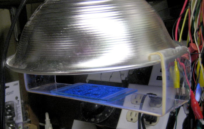 Update 3/24/13: I’ve been using the little blacklight bulb in the 8″ polished reflector for all my PCB exposures for over a year now, and it’s just great. I made up a quick and dirty board support from a scrap of clear acrylic that hooks over the edges of the lamp to provide constant
 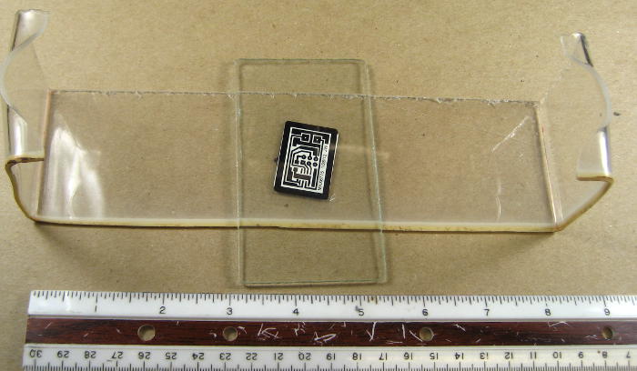 distance from board to bulb/reflector with minimal effort. Here it is with the usual sandwich of board, artwork (ink side down) and glass on top to hold the artwork in intimate contact with the board.
Also, driven by a need to produce a couple of prototype boards for Workshop88’s THOTCON badges, I tuned my process to give very consistent excellent results with 10 mil traces – which I’d never even attempted before. The test artwork was 10 mil wide lines on 20 mil centers. Success was exactly equal line/space widths after etching. The final result was reducing the exposure time (with exactly the setup above) to one minute and 40 seconds. Comes out perfect every time.