
Thanks to some urging from Steve S, we finally got geared up to try PCB drilling on the Shapeoko 2 at the space last Thursday (8/13/15). (We had planned to use it to drill badge boards last September, but during initial accuracy verification we found it was off by a lot – 0.1″? – over 8 inches or so. I was shocked, but we didn’t have time to troubleshoot it, and so bought a couple of Dremel drill presses and drilled all the boards by hand. SO2 PCB drilling dropped out of view after that.) The first test for Steve was again accuracy verification. But this time it was over just a few inches, so I was pretty confident it would be OK.
We rediscovered that we used the pcb-gcode User Level Program in Eagle to generate drill gcode. We downloaded the latest version, rediscovered how to use it, generated some gcode, and were ready to test.
Well, almost. Since we wanted to drill from the bottom (foil) side of the board, we discovered that the gcode generated for a bottom drill was mirrored in X, with all values negative. Bill, Steve and I did a LOT of talking and waving our hands around trying to get our heads around the problem and find a solution. We finally did so, and after a couple of air-drills, mounted a #64 carbide bit and actually drilled the holes for Steve’s test adapter board in foam. There’s little question that the machine can actually drill PCB material, so all we needed from the foam was an accuracy test.
It passed! 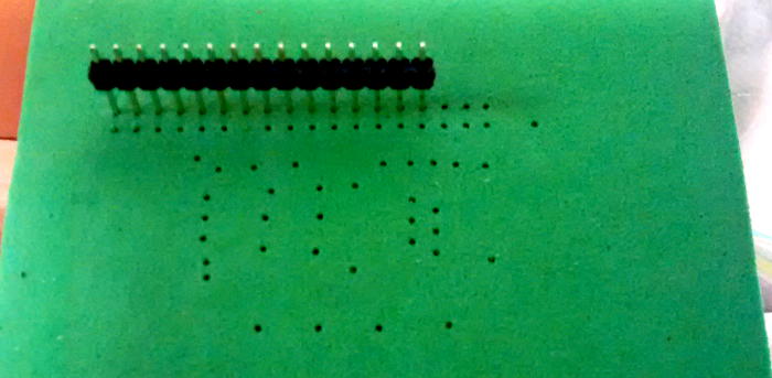 A piece of 0.1″ header – a quite accurate ruler/test gauge that’s always around – fit the holes for a header very well. Steve didn’t have an etched board to drill, but went home happy with the accurately drilled foam for show and tell.
Nanino and the dreaded scale error
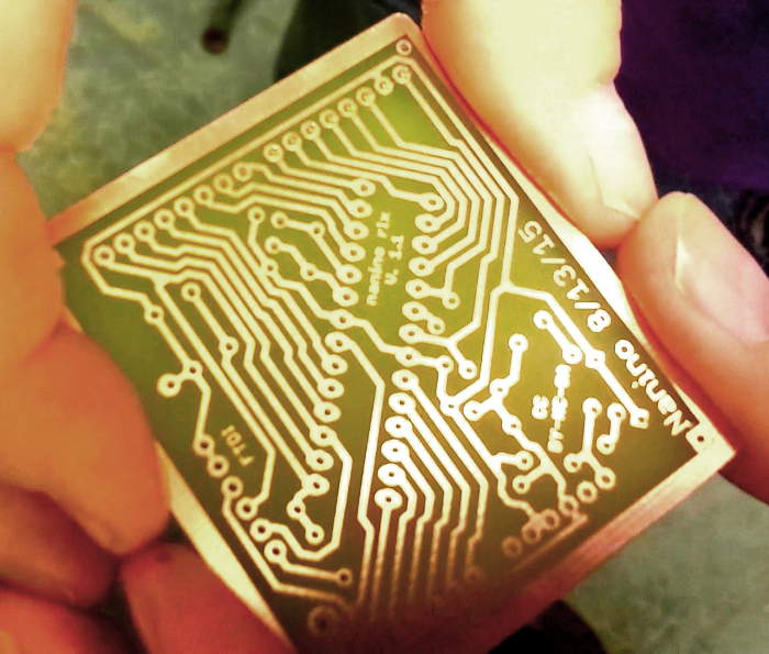
I was pretty confident that once we could get good gcode the SO2 would work, and wanted to bring a board we could actually drill that night. I found a nice minimal, single sided Arduino (no USB chip) called Nanino. I downloaded the Eagle files (thanks, robelix!), made up the board as usual, and it looked fine. Or so I thought. We generated the gcode, did the magic X axis inversion, used one of the fiducials I’d cleverly included in the corners of the board to set, jog, and reset workpiece home. Just to be sure, we jogged to the opposite fiducial – and it was off – by more than 50 thousandths! WTH? We did lots of measurements, including with a digital caliper and the venerable 0.1″ header as ruler. The problem was that board was just slightly too big. And by enough that holes didn’t have a prayer of lining up all over the board. We gave up on the board and went home.
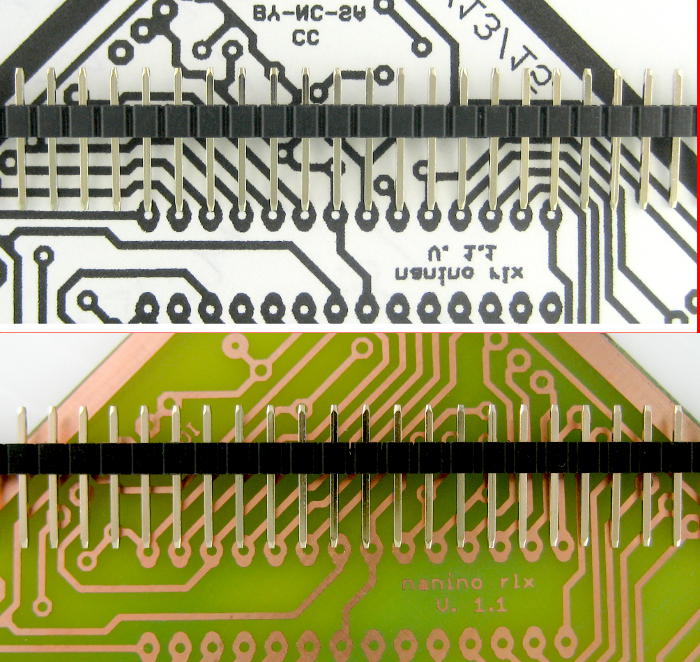 At home the next day, I did some more checking. The check plot on paper – which I always do to make sure it’s placed correctly before printing the artwork on clear film – was much closer. You can see the comparison on the left. (The check plot is reversed wrt the board.)
This is the third time I’ve had boards come out the wrong size – but close enough to not be caught until it was almost time to populate the board. The first was with latch boards for the never-finished scrolling LED display I inherited from Rich, Inc. The second, and most expensive, was some 40 badge boards that got etched and some drilled 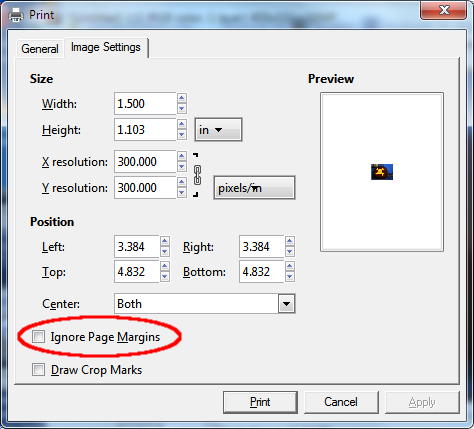 before we found it. As I recall, at least one of those first 2 was due to some arcane print setting in gimp. By ignoring or not, it decided to scale to fit the page under some rare circumstances.
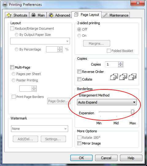 This one turned out to be similar: In the Epson custom PCB printing settings I’d recreated after somehow losing them, I’d selected “Borderless prints”, which enabled some arcane “Enlargement” feature. When I set that to “Retain Size” instead of “Auto Expand”, my plots using the custom PCB settings came out the same size as the check plots (which used default document settings that didn’t fall prey to “Enlargement”). I resaved those settings as “PCB 2”, printed new artwork, and made up a new board. This time a header actually lines up with the pads!
Drilled and working Nanino!
 I took the board to the space, did all the magic setup and rechecked the far fiducial. It was right on!
 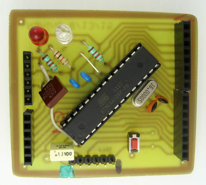 We drilled a piece of paper, and the holes lines up with the board beautifully. We drilled the board, and it looked great – probably better/more consistent than I could do by hand on the drill press. (Sorry for only a fuzzy video screen snapshot.) I stuffed and soldered the board, and got a working Arduino! Although it doesn’t have an ICSP header, it’s still a very usable Arduino. I’ve already tested it with strandtest and some Neopixels, and it works fine.
Gory registration details (updated)
A critical setup step to getting holes drilled in the right places is how to register the board so the X,Y coords in the gcode match the physical board. Pcb-gcode will provide either or both top drill or bottom drill gcode files, and we chose to drill the board from the foil side – the ‘bottom’. That adds an extra layer of obfuscation, since Eagle’s view is always from the top of the board. I used Universal Gcode Sender to talk to the SO2’s Arduino running (hacked) grbl0.9g., so the instructions below are with that tool in mind.
I laid out a registration hole in each corner, such that the 2 holes along each edge changed only the X or the Y value. That proved very valuable, though any 2 holes fairly far apart and whose Eagle coordinates were known would have worked.
Since we’re drilling from the foil side, the ulp rotates the board around the Y axis at X=0. It picks the far right edge of the board up and flops it over into negative X space so you’re looking at the bottom of the board. If the bottom edge of the board used to go from say X=0.2 to X=3, it will now reside at X=-0.2 to X=-3. The Y coordinates are unchanged, but all the X coordinates are the same values, but negative (assuming they were all positive to begin with). Knowing that the hole in the corner nearest the N in Nanino was at -o.85,0 and the second was at -2.7,0, I tried the following steps (now simplified using G92)and they worked. This all assumes the board is accurately horizontal so if the bit is just clear of the surface at one point it will be just clear of the surface at any other point!
How and where we locate the board needs to reflect the X-axis mirroring we get by drilling on the foil side. Say the board is 3″ wide. Looking from the top/component side, some corner (call it the ‘home’ corner) will be near 0,0 in Eagle coordinates. Instead of being near the corner of the plastic registration guides on the SO2, when viewed from the foil side, the ‘home’ corner will be out in the middle of the spoil board – maybe 3″ or 4″ to the right of the registration guide corner. Nothing changes for the Y axis.
Place the board so the ‘home’ corner is off to the right and near the “bottom”/X axis plastic guide, and the left edge is comfortably clear of the far left registration guide.
BOARD REGISTRATION STEPS:
– Locate the board comfortably on the base and temporarily tape it down. I used a corrugated cardboard spoil board under the PCB.
– Manually position drill bit precisely over one known hole (here, the one at -0.85, 0).
– Drill the hole using the UGS jog controls. Drill into the spoil cardboard. Raise the bit to barely clear the surface – maybe 0.5mm. This will be Z=0.
– In the UGS Command tab, manually enter gcode to set the workpiece coord system to match the coords of this hole. Because we’re drilling the foil side, all the X coordinates – including this hole – are NEGATIVE – so be sure to reflect that. For our first hole, that gcode would be: G20G92X-0.85Y0Z0. Never move the gantry by hand after this!
– Raise the bit up with the jog controls to give you access to the hole – maybe 2″.
– Now insert a pin (0.39″ diam rod or wire would be nice, but a 0.025″ square pin will do) thru the hole in the board and into the spoil board. Gently untape the board. At this time, the board and the machine’s coord system match at that one hole.
– Manually enter gcode to move to the absolute X,Y coords of another known hole and say 0.05″ above the surface. Here that hole was at -2.7,0. (G20G90G0X-2.7Y0Z0.05) Going to Z=0 is risking the bit.
– Carefully rotate the board around the pinned first hole until the second hole is exactly below the bit. If you can’t get it exactly below, you have some other problem! At this point, your board is exactly in position.
– Tape or clamp the board down securely, and recheck the second hole. Pull the pin out of the first hole. You should be ready to go!
I hope that conveys what it took us a fair bit of time to become comfortable with. I think Bill said he even found doc that corroborated what we’d figured out.
PCB design rules
Since we had some issues with how Steve’s board was designed – trace and clearance widths and hole sizes in particular – I’ll abuse this space to start collecting PCB design rules for the photo process (I and) Workshop 88 uses. Folks accustomed to sending designs out to board houses think in term of different limitations than our homebrew PCB system requires. Some of this is “how I’ve always done it”; some is what I think we can/can’t get away with. Yeah, I suppose they could be entered into a design rules file, and while that’s exactly what the DRC is for, that seems somehow excessive for a hacker process. But that’s probably just me.
Trace widths
My usual practice is 16 mil traces, with 24 or 32 mils for power and ground. The photo process can handle those traces on a bad day, with a headwind, and when your timing’s off. 16 mils is way overkill for the current carried by most any Arduino-class project. I’ve done 12 mil with little difficulty, and even a few 10 mil sections under duress. And the 8 mil (!) traces on Steve’s board came out looking quite good, so my 16 mil traces remain VERY conservative. I’m unlikely to change that standard.
Clearance between traces
I almost always leave (at least) 16 mil clearance between traces. Again, this is very conservative for a well-tuned process. I guess I’d have to say that 12 mils was quite safe. I’d start getting uncomfortable with anything less, tho.
Other clearances
I also try for 16 mil clearance between anything else – traces and the corners of pads, between pads, etc. Since there are most aways some nice 16 mil traces nearby, it’s pretty easy to eyeball that clearance. I guess I’d get uncomfortable with anything under 12 mils. Obviously some SMT components force smaller clearances than that. You do what you’ve gotta do.
Hole sizes
A perennial problem with component footprints from imported libraries is that the holes in the pads are too big. I drill almost everything with a #64 (carbide) bit (0.039″), and if the hole in the pad is bigger than that (or even if it’s that size and I miss centering the hole a little), there will be an unsolderable gap between the pin and the copper pad. I never want the process to make soldering more difficult than necessary.
I’ve redefined many parts so the pads have the smallest offered drill size – maybe 0.019″. All the new footprints I make have those holes. That way there’s a nice small target if I’m drilling by hand; the small hole helps center the bit; and there’s always copper all the way to the edge of the hole.
A possible downside would be if drilling with the Shapeoko and if the hole location and drill bit location didn’t exactly match, the centering effect of the hole might exert a lateral force on the bit, potentially breaking it. I’ve never seen this happen, but I’ve only drilled a very small number of boards.
Pads and vias
I often use oblong pads to give a little more copper to solder to while increasing the space between pads in case I have to put a trace thru there. By using oblong pads with holes near one end, I can get a little more space “down the middle” of dual row 0.1″ headers. When I need a jumper, I use a via. I try to make it 0.07″ or even 0.086″ so I have a fair place to solder to. As always, holes are as small as possible.
Single sided prototypes for designs ultimately to be sent to a board house
I’ve made single sided boards as prototypes for designs I want to send to a board house, and had fairly good luck. I try to minimize the number of traces on the back of the board, and use my oversize vias for the jumpers. I route the trace on the other side of the board in Eagle, so I have indication where the jumpers go (although I obviously turn off the layer for that side of the board when printing).